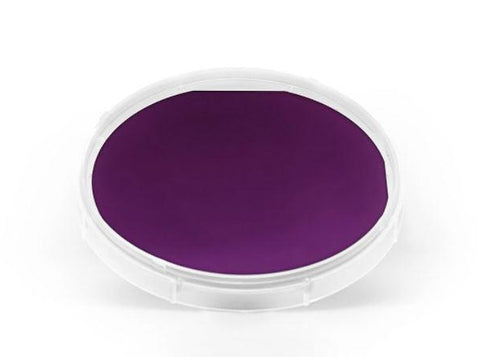
Silicon/Silicon Dioxide (Si/SiO2) 300nm Wet Thermal Oxide Silicon Wafer and Substrates, Prime Grade
SKU: SU3801
Thermal oxide (silicon dioxide, SiO2) layer is formed on silicon wafer surface at an elevated temperature in the presence of an oxidant. This process is commonly referred to as a thermal oxidation process. The SiO2 thermal oxide thin film is normally grown in a horizontal tube furnace, at temperature range from 900°C ~ 1200°C.
Silicon/silicon dioxide (Si/SiO2) thermal oxide wafers and substrates are widely used for FET substrates, surface microscopy analysis, ellipsometry measurements and X-ray studies. MSE Supplies also offers monolayer graphene film on Si/SiO2 substrate. (10mm x 10mm, 1 inch x 1 inch, and more...)
We can offer a variety of choices for customization. Please contact us at sales@msesupplies.com for your requirements of customized products.
MSE Supplies offers the following choices:
- Type of silicon wafer: N or P type
- Silicon wafer doping: un-doped, P-doped or B-doped
-
SiO2 thickness: 300~500 nm. The standard thickness is 300 nm.
- Electrical resistivity: un-doped (>1000 Ωcm), P or B doped (10-3~104 Ωcm)
- Crystal orientations: (100), (111) and (110)
- Substrate sizes: 10x10 mm, 15x15 mm, 2", 3", 4" or customized
- Thickness: 0.3~0.5 mm, 1.0 mm or customized
- Surface polishing: Single Side Polished (SSP) or Double Side Polished (DSP)
|
Properties |
|
| Crystal Structure of Si | Face-centered cubic |
| Melting Point | 1410 ℃ |
| Density | 2.4 g/cm3 |
| SiO2 Thermal Oxide Film Thickness | 300 nm |
| EPD | ≤100∕cm2 |
| Oxygen Content | ≤1~1.8 x 10^18 atoms/cm3 |
| Carbon Content | ≤5 x 10^16 atoms/cm3 |
| Size Tolerance | <±0.1mm |
| Thickness Tolerance | <±0.015mm or <±0.005mm upon request |
| Wafer Orientation Precision | ±0.5° |
| Edge Orientation Precision | 2° (1° if requested) |
| Packing | Packed with class 100 clean wafer case or bag in a class 1000 cleanroom |
