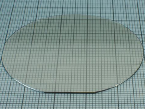
2 inch Ammonothermal High Electron Concentration N-type Free-Standing Gallium Nitride (GaN) Substrate
SKU: WA0257
2 inch Ammonothermal High Electron Concentration N-type Free-Standing Gallium Nitride (GaN) Substrate
Free-Standing Gallium Nitride (GaN) is a promising wide band gap material. There are two main ways to produce them, Hydride Vapour Phase Epitaxy (HVPE) and ammonothermal. HVPE has a faster growth rate and a larger sized substrate which can be produced up to 4". Ammonothermally grown substrates have relatively low growth rates and a size of up to 2". Despite the lower growth rates and smaller sizes ammonothermally grown substrates have excellent structural properties and low dislocation density. These superior properties allow researchers to discover more advanced applications. Similar to all free-standing GaN, it can be used in various applications, including power devices, RF devices, laser diodes and LED.
Conductivity type: N-type, Oxygen Doped
- Dimension: 49 +/- 0.5 mm (WA0257) / 50.4 +/- 0.5 mm (WA0258)
- Thickness: 430 +/- 50 um
- Primary Flat: 14 +/- 1 mm (WA0257) / 16 +/- 1 mm (WA0258)
- Secondary Flat: 8 +/- 1 mm
- Orientation: (0001) C-plane
- Total Thickness Variation: ≤ 60 um
- Bow: 0 +/- 20 um
- Resistivity: ~ 10-3 ohm.cm
- Carrier Concentration: ~ 1019 cm-3
- Carrier Mobility: ~ 150 cm2/V*s
- FWHM (0002), epi-ready surface at 100 um x 100 um slit: ~ 20 arcsec
- Etch Pit Density: < 5 x 104 cm-2
- Polishing: Front surface: RMS < 0.5 nm, Epi ready, Back surface ground.
- Growth Method: Basic ammonothermal method with T ~ 650 °C.
*The picture shown might be different from the actual product.
Customization:
Customized GaN Free-Standing products can be made to meet customer's particular requirements and specifications.
References:
- GaN-on-GaN pn power diodes with 3.48 kV and 0.95 mΩ-cm2: A record high figure-of-merit of 12.8 GW/cm2. In 2015 IEEE international electron devices meeting (IEDM), pp. 9-7. IEEE, 2015.
- High voltage, high current GaN-on-GaN pn diodes with partially compensated edge termination. Applied Physics Letters113, no. 2 (2018): 023502.
