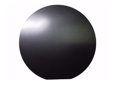
MSE PRO 4 inch Silicon-on-Insulator (SOI) Wafer (Device: 10μm; Box: 2μm)
SKU: WA2601
MSE PRO™ 4 inch Silicon-on-Insulator (SOI) Wafer (Device: 10μm; Box: 2μm)
Silicon-on-Insulator (SOI) wafer is a structure including the device layer (top), buried oxide layer (middle), and handle wafer (bottom). This technology allows for the continuous miniaturization of microelectronic devices. It has several advantages over a traditional silicon wafer, like low leakage currents and parasitic capacitance. It is used in various applications, including MEMS, sensors, telecommunications, and power devices. For example, the researchers at Toyota Central R&D Labs proposed simple T-shaped support as a solution to the tilt deformation caused by the residual stress. This solution could potentially allow for the development of high-precision sensors and actuators.
Specification:
| Parameter | Specification Range |
| Diameter | 100 ± 0.5mm |
| Device Layer | |
| Thickness | 10 ± 0.5 μm |
| Type/Dopant | N / Phosphorous |
| Orientation | (100) ± 1 deg |
| Resistivity | <0.005 ohm.cm |
| Box Layer | |
| Thickness | 2 μm ± 10% |
| Handle Wafer | |
| Thickness | 400 ± 10 μm |
| Orientation | (100) ± 1 deg |
| Type | N / Phosphorous |
| Resistivity | 0.01-0.05 ohm.cm |
| Backside | Polished with oxide and lasermark |
| Quantity | 1 piece |
*The figure is for reference only. The actual product may look different due to configuration difference.
Please contact us for customized SOI wafer.
References:
