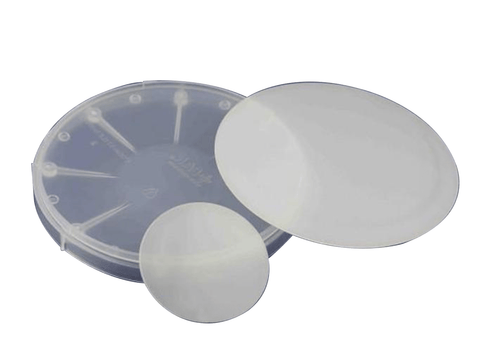
MSE PRO 4 inch N-Type Undoped GaN 4 um Gallium Nitride Template on Sapphire (0001)
SKU: WA0213
4 inch GaN Templates on Sapphire (0001), N-type (undoped), GaN 4 um
- Product SKU#: WA0213
- Conductivity type: N-Type (undoped)
- Dimension: 100 mm +/- 0.1 mm (4 inch diameter)
- GaN Thickness: 4.5 +/- 0.5 um
- Usable area: >90%
- Orientation of GaN: C plane (0001) off angle toward A-axis 0.2 ± 0.1
- Primary Orientation Flat of GaN: (1-100) +/- 0.2 deg, length 30.0 +/- 1.0 mm
- Total Thickness Variation (TTV): <25 um
- Resistivity (300K): < 0.5 Ohm-cm
- Dislocation Density: < 5x10^8 cm^-2
- Carrier concentration (~ doping concentration): > 2x1018 cm-3
- Mobility > 200 cm2/V-s
- XRD FWHMs: (0002) < 300 arcsec, (10-12) < 400 arcsec
- Surface AFM RMS: < 0.5 nm
- Sapphire substrate thickness: 650 +/- 25 um
- Orientation of sapphire substrate: C plane (0001) off angle toward M-axis 0.2 ± 0.1, length 30.0 +/- 1.0 mm
- Substrate Structure: GaN/Sapphire (0001)
- Polishing: single side polished (SSP) is standard, double side polish is available upon request.
- Package: packaged in a class 100 clean room environment, in single wafer containers.
Related references:
1. Electrical Characteristics and Deep Traps Spectra of Undoped GaN Films Grown on Si Using Different Strain-Relieving Buffer Types
DOI: 10.1109/TNANO.2013.2294996
Abstract:
Electrical properties of GaN films grown on Si by molecular beam epitaxy using various types of strain-relieving layers have been studied by means of Hall/van der Pauw measurements, capacitance-voltage profiling, admittance spectroscopy, and deep levels transient spectroscopy with electrical and optical injection. The electrical properties of all grown films were determined by relatively deep electron traps N1, N2, and N3 with aggregate concentration of ~1017 cm-3. Freezing out of these traps led to the films freezing out down to the depth corresponding to the nearest underlying heterointerface where a strong band bending caused a sharp nonuniformity of charge carriers concentration. For AlN or Al-rich AlGaN underlying films, this band bending could cause formation of hole sheet charge leading to apparent conductivity to appear p-type in Hall. Other deep traps detected in the grown films were N4 and N5 acceptors with levels near Ec - 0.6 eV, and hole traps H1 and H2 with levels near Ev + 0.9 eV. Possible consequences of the observed phenomena for designing the thick GaN stand-off films in power transistors are briefly discussed.
