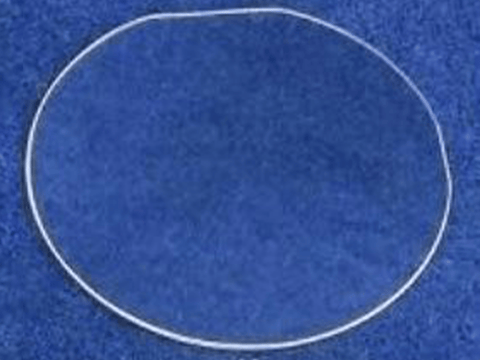
MSE PRO Dummy Grade 2 inch Si-doped N-type Gallium Nitride Single Crystal C plane (0001)
SKU: WA0210
Dummy Grade Free-standing GaN substrate, C plane (0001), size 2" diameter
- Dimension: 2" diameter
- Thickness: 400 +/- 30 um
- Usable area: ≥70%
- Orientation: C plane (0001) off angle toward M-axis 0.55+/- 0.15 deg
- Flat: (1-100) +/-0.1 deg, 12. 5+/-1 mm
- Total Thickness Variation: ≤15 um
- Bow: ≤20 um
- Resistivity (300K): ≤0.02 ohm.cm
- Carrier Concentration: 1-2 E18 cm-3
- Dislocation Density: ≤ 3 x 106 cm-2
- Polishing: Front surface: Ra ≤0.3 nm, Epi ready, Back surface fine ground.
- Package: packaged in a class 100 clean room environment, in single wafer container, under nitrogen atmosphere.
Related References
1. GaN-based light-emitting diodes on various substrates: a critical review.
doi: 10.1088/0034-4885/79/5/056501
GaN and related III-nitrides have attracted considerable attention as promising materials for application in optoelectronic devices, in particular, light-emitting diodes (LEDs). At present, sapphire is still the most popular commercial substrate for epitaxial growth of GaN-based LEDs. However, due to its relatively large lattice mismatch with GaN and low thermal conductivity, sapphire is not the most ideal substrate for GaN-based LEDs. Therefore, in order to obtain high-performance and high-power LEDs with relatively low cost, unconventional substrates, which are of low lattice mismatch with GaN, high thermal conductivity and low cost, have been tried as substitutes for sapphire. As a matter of fact, it is not easy to obtain high-quality III-nitride films on those substrates for various reasons. However, by developing a variety of techniques, distincts progress has been made during the past decade, with high-performance LEDs being successfully achieved on these unconventional substrates. This review focuses on state-of-the-art high-performance GaN-based LED materials and devices on unconventional substrates. The issues involved in the growth of GaN-based LED structures on each type of unconventional substrate are outlined, and the fundamental physics behind these issues is detailed. The corresponding solutions for III-nitride growth, defect control, and chip processing for each type of unconventional substrate are discussed in depth, together with a brief introduction to some newly developed techniques in order to realize LED structures on unconventional substrates. This is very useful for understanding the progress in this field of physics. In this review, we also speculate on the prospects for LEDs on unconventional substrates.
2. Advantages of Employing the Freestanding GaN Substrates with Low Dislocation Density for White Light-Emitting Diodes
http://global-sei.com/technology/tr/bn75/pdf/75-21.pdf
To improve the luminous efficiency of white light-emitting diodes (LEDs) for general lighting, the InGaN-based-LEDs with thick quantum wells (QWs) were examined on our unique freestanding gallium nitride (GaN) substrates with lowthreading dislocation densities (TDDs). With LEDs grown on sapphire, which are commonly used, the crystalline quality of QWs was deteriorated and the luminous efficiency was degraded with the increase in the total thicknesses of InGaN QWs. On the other hand, on the GaN substrates with low TDD, the luminous efficiency at high current density was successfully improved without the deterioration of crystalline quality as the total thicknesses of InGaN QWs increased. Consequently, it was confirmed that the combination of thick InGaN QWs and low-TDD GaN substrates gives rise to highly efficient LEDs required for solid state lighting. Keywords: LED, droop, GaN, InGaN, GaN substrate, dislocation,
